
Reference | All - Docs - Libraries - Soft Processors - Cores
8-bit DAC IP Core with Wishbone Interface
Author
Jestoni
Introduction
The 8-bit DAC IP core is integrated to the Arduino soft processor for Papilio which is based on the ATmega168 processor. This IP core is designed to be a peripheral to the soft core with its own I/O address space. With this IP core, the Papilio can read sound files from the SD card and send it to the DAC to produce the desired sound waves.
The detailed discussion of the base DAC IP core can be found here, http://www.xilinx.com/support/documentation/application_notes/xapp154.pdf. What I did was to interface this IP core to the Arduino soft processor using Wishbone interface. The maximum sampling rate of the DAC IP core was also considered.
Hardware Description
Figure 1 shows the top level block diagram of the peripheral that will be attached to the soft core. It has the default pins of the papilio_core_template plus the additional pin, DACout, which is the actual output of the DAC. The description of each pin are tabulated in Table 1. This peripheral has an IO address equal to 8bit hex == “E0”. This can be easily change by modifying the DAC_lib.vh include file, set the correct address at the io_base_address_DAC variable.
| Pin Name | Direction | Description |
|---|---|---|
| Adr[7:0] | input | To transfer data to the DAC core, adr should be equal to the io_base_address assigned for the DAC IP core. To select the status of the DAC, adr should be io_base_address plus one. |
| Dbus_in[7:0] | input | Contains the data to be converted. |
| clk | input | Main clock |
| iore | Input | Read enable signal |
| Iowe | input | Write enable signal |
| nReset | input | Global reset. (Normally ‘1’) |
| Dbus_out[7:0] | output | Contains the status of the DAC core. |
| DACout | output | Contains the converted serial data. |
| Out_en | Output | Asserted when the DAC completes one sampling cycle (256 clock cycle) |
Table 1 Pin Description of the Papilio Core Peripheral
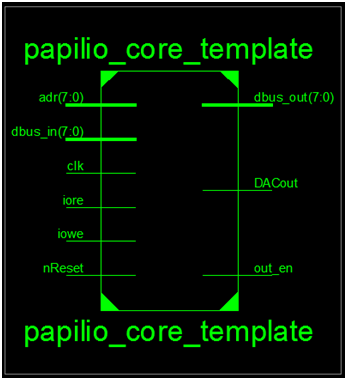
Figure 1 Top Block of the Papilio Peripheral
Figure 2 shows the three major blocks of the IP core, first is the AVR2DACWishbone_bridge. This is the Wishbone master interface where the controller of the wishbone handshake is located. Next is the DAC_wb which is the Wishbone slave block for the DAC. The third one is the actual DAC which is the IP core described in the application app previously mentioned.
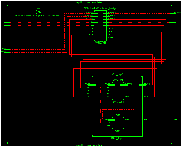
Figure 2 Major Blocks of the IP Core
Wishbone Slave
A simple 8-bit interconnect wishbone was used in this IP core. The reference design is illustrated in Figure 3
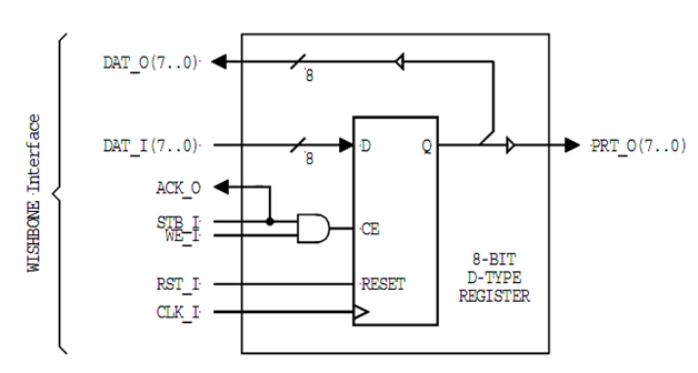
Figure 3 Simple 8-bit Wishbone Slave Output Port
One of the major change that was added in this Wishbone slave is the counter that sets if the DAC core is busy or not. The actual value of the input data is equivalent to the average duty cycle for one sampling which is has a minimum value of 2^(number of input bits) == 256. Basically the output of the DAC is inaccurate before 256 clock cycles. Thus, a counter was added to the slave wishbone which controls the ACK_O signal.
The schematic of the busy block is shown in Figure 4. The main instance in this block is the 8-bit counter where the output is ANDed to set the ACK_O signal. The clear signal of the counter is controlled by the two D-flipflop, inside the white box. It act as a edge detection circuit. It detect the positive edge of the iowe signal from the top block and sends a single pulse to the counter to start the counting. The edge detection circuit was chosen so that the iowe can have variable length and will not affect the counter since it is edge detected only. The DFF inside the yellow box is the clock controller. It stops the clock, which in turn stops the counting, once the counter reach 255.
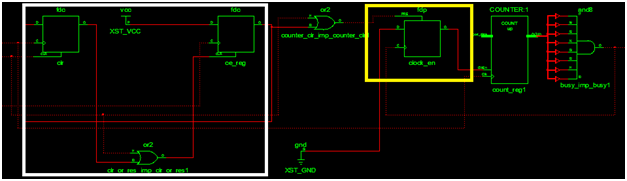
Figure 4 Schematic of the Busy Block
System Flowchart
Figure 5 shows the system flowchart of the DAC IP core interface to the Arduino soft core. These are the steps necessary to communicate to the DAC IP core. First step is the initialization of the signals like clk, res and other signals. Then set the signal to io_base_ddress_DAC+1 to access the status of the DAC core. The iowe signal is also set to 1’b0 (one bit data which is equal to zero) at this point. If the DAC IP core is ready, dbus_out will be equal to 8’h01 (8 bit hex data which is equal to 01) else it is 8’h00.
Next step is to set the adr to io_base_address_DAC to access the register of the DAC. Also set the input data with the address. When the iowe is set to 1’b1, the data in the dbus_in will be written to the DAC register.
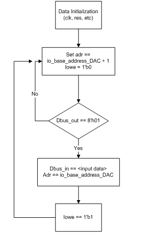
Figure 5 System Flowchart
Test Bench
The testbench for the whole IP core is located at the tb_DAC.v file. It has different task module that exercise the different scenario for the design. The test bench is well documented and can be used as a reference.
Test Waveforms
Figure 6 shows the initialization of the transfer to the DAC core. Notice that even if the DACready (blue signal) is already ‘1’, the dbus_out is still equal to zero. This is because the adr signal is not equal to io_base_address_DAC + 1 == 8’he1. So when the adr is set to 8’he1, the dbus_out signal turns to 01 which tells the processor that the DAC is ready to accept new data. New data is place in the dbus_in and the adr is set to io_base_address_DAC == 8’he0 directly after the detection. Then a single pulse of iowe starts the transfer and the counter of the DAC core which sets the DACready to zero.
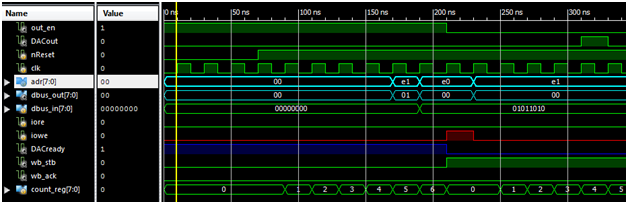
Figure 6 Initialization of the Transfer Protocol
Figure 7 shows what happens when the counter finished counting up to 255. The wb_ack asserts when the counter finished counting. Notice that the wb_stb signal is asserted all throughout the transfer, it is only deasserted once the ack is equal to 1’b1. The next transaction is immediately initiated to show the reaction of the DAC core.
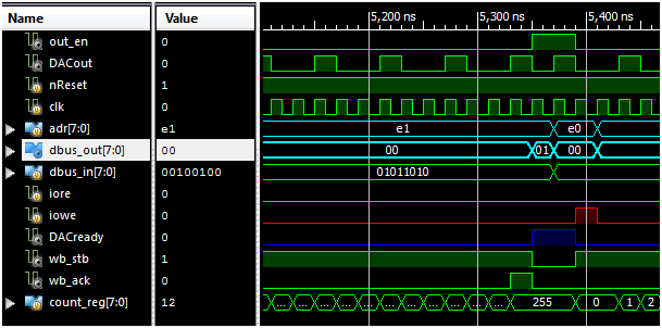
Figure 7 End of a Conversion
Figure 8 shows the top level simulation results once the tb_DAC.v is simulated. Basically this tests emulates different length of iowe signal. It can be seen from the waveforms that the DAC core react properly and the DACout differs with every change in dbus_in.
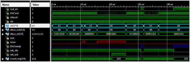
Figure 8 Top Level Simulation Results